Wave Computing offers machine learning platform
The machine learning compute appliance executes dataflow graphs using multiple clock-less, CGRA-based system chips (SoCs), or dataflow processing units (DPUs), each containing more than 16,000 processing elements (PEs).

Microarchitecture of a 6.7GHz Processing Element (PE). Source: Wave Computing.
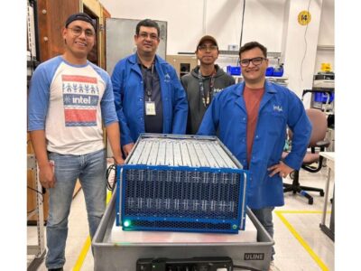
Wave Computing claims that one of its compute appliance units can deliver up to 2.9 peta operations per second of performance by using 16 DPUs (256,000 interconnected PEs), more than 2 terabytes of bulk memory and high-speed HMC memory, as well as up to 32 terabytes of storage. Up to four Wave compute appliances can be combined within a single node in a data center.
The compute appliance, which is based on dataflow processing SoCs or DPUs developed by Wave, natively executes dataflow graphs to speed up neural network training compared with other systems. It also enables support for much larger datasets in a single data center node. Wave is offering access to compute appliance prototypes before system sales begin in Q4 2017.
Wave Computing was founded as Wave Semiconductor Inc. by Peter Foley, an entrepreneur in residence at Tallwood Ventures and Karl Fant. Fant had previously founded Theseus Logic to commercialize a form of asynchronous logic called Null Convention Logic.
The company changed its name in 2016 and is now led by Derek Meyer, CEO, and Chris Nicol, CTO.

Cluster of 16 PEs with 8 Arithmetic Units, Source: Wave Computing.
The DPU chip is essentially an FPGA-style array SoC of clockless processing elements (PEs). It contains 16,384 PEs configured as a coarse-grained array (CGRA) of 32 by 32 clusters of 16 PEs. The chip includes four hybrid memory cube generation 2 interfaces, two DDR4 interfaces, a PCIe Gen3 16-lane interface and an embedded 32bit processor for SoC resource management. The identity of the housekeeping RISC has not been identified but CEO Meyer, was previously employed at MIPS, Ceva and ARC. ARC was subsequently bought by EDA compay Synopsys.
Next: Chip is done, next chip design started
Wave stresses that the DPU is not coprocessor but executes autonomously with a small host only used for initiating program loading, runtime reconfiguration, check-pointing and the like.
Chris Nicol, CTO, said in LinkedIn: “Chip is done. Tools are done. Now for the systems… Next chip is already underway. We are hiring!!’

CGRA configured as a mesh of 32×32 clusters, and partitioned into 24 machines. Source: Wave Computing.
The CGRA architecture is a mesh of locally connected PEs with the tool flow mapping a high-level program across multiple processing elements. It is Wave’s conclusion that CGRAs offer greater flexibility and performance than FPGAs for machine learning applications.
To ease the execution of dataflow graphs from machine learning workflows, such as Google’s TensorFlow, Wave has developed the WaveFlow software framework. This is a library of neural network models that the WaveFlow session manager instantiates into the DPU chips at runtime. Robust processing of tensors is achieved without the need for a host CPU or runtime API such as CUDA or OpenCL. Initially supporting TensorFlow, future releases are planned to support Microsoft’s Cognitive Toolkit (CNTK), MXNet and others.
Related links and articles:
News articles:
Self-timed logic is Eta Compute’s low-power secret
Graphcore’s execs on machine learning, company building
EE Times Silicon 60: 2016’s Emerging Companies to Watch
 If you enjoyed this article, you will like the following ones: don't miss them by subscribing to :
eeNews on Google News


