PCM memory is programmable by photons and electrons
Developed in Harish Bhaskaran’s Advanced Nanoscale Engineering research group in collaboration with researchers at the universities of Münster and Exeter, the electro-optical device bridges the fields of optical and electronic computing and could in the future provide an elegant solution to achieving faster and more energy efficient memories and processors.
Publishing their results in Science Advances under the paper title “Plasmonic nanogap enhanced phase-change devices with dual electrical-optical functionality”, the researchers explain how they combined waveguide-integrated plasmonic nanogaps with Ge2Sb2Te5 (GST) as a photo- and electro-sensitive phase change material to create an electro-optic memory cell that is fully addressable in both electrical and optical domains.
While electrical chips need to be small to operate efficiently, optical chips usually need to be large as the wavelength of light is larger than that of electrons, making electrical and light-based computing fundamentally incompatible. It is by exploiting both the nanoscale dimensions and strong field confinement of a plasmonic nanogap that this full mixed-mode operation was enabled, switching the amorphous/crystalline states of the PCM within a 50nm gap.
The dramatic size reduction in conjunction with the significantly increased energy density achieved in this electro-optic memory cell is what allowed the researchers to bridge the apparent incompatibility of photons and electrons for data storage and computation. More specifically, they demonstrated that by sending either electrical or optical signals, the GST nanogap was transformed between two different states of molecular order, which could be read out by either light or electronics thereby making the device the first electro-optical nanoscale memory cell with non-volatile characteristics.
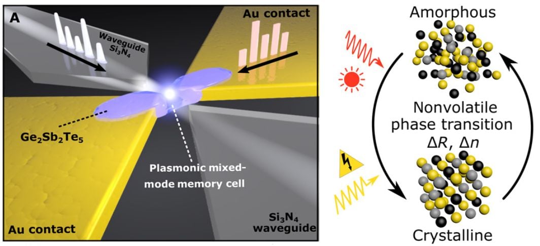
nanoscale device via a photonic waveguide, while the Au
contacts serve as both device electrodes and plasmonic
nanogap (50nm) to focus incoming light.
Optical programming of the PCM memory cell is performed with optical write and erase pulses that partially amorphize and crystallize the GST within the nanogap. Likewise, electrical write and erase pulses can be used to switch the GST between its amorphous and crystalline states, which can then be read out both optically and electrically by monitoring the material’s optical transmission and electrical resistance simultaneously.
“This is a very promising path forward in computation and especially in fields where high processing efficiency is needed” said Nikolaos Farmakidis, graduate student and co-first author of the paper.
“This naturally includes artificial intelligence applications where in many occasions the needs for high-performance, low-power computing far exceeds our current capabilities. It is believed that interfacing light-based photonic computing with its electrical counterpart is the key to the next chapter in CMOS technologies”, added co-author Nathan Youngblood.
University of Oxford – www.ox.ac.uk
Related articles:
Academics scale PCM with carbon nanotubes
IBM reports drift-tolerant multilevel cell PCM
IBM uses phase-change memory for machine learning
CEO interview: Nantero’s Schmergel says NRAM production is close
 If you enjoyed this article, you will like the following ones: don't miss them by subscribing to :