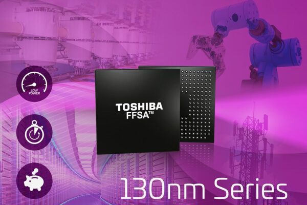
130nm Fit Fast structured array development platform
Using an innovative approach, all FFSA devices have a common silicon-based master layer that is used in combination with upper metal layers that are reserved and allow device customization.
The FFSA platform meets customer requirements for high performance and low power consumption; however, by limiting the customization to just the metal layer masks, it also reduces development cost drastically. As a result, samples and mass-produced devices can be delivered in a significantly shorter time than for conventional ASICs. Customers using the FFSA ASIC design methodology and library secure higher performance and lower power consumption than is possible with Field Programmable Gate Arrays (FPGAs).
The new FFSA 130nm process is added to Toshiba’s current 28, 40, and 65nm process portfolio adding another option for industrial equipment. The 130nm node process offer different master slices for up to 664kb of RAM and around 912,000 gates per device.
Devices designed on the platform will be manufactured by Japan Semiconductor, a subsidiary of Toshiba Electronic Devices & Storage Corporation with a long and proven track record of expertise in manufacturing ASIC, ASSP and microcomputers.
Toshiba Electronics Europe – www.toshiba.semicon-storage.com
 If you enjoyed this article, you will like the following ones: don't miss them by subscribing to :