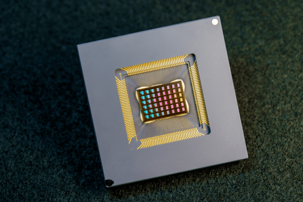
48 core neuromorphic AI chip uses resistive memory
A team of researchers in the US and China has designed and built a neuromorphic AI chip using resistive RAM, also known as memristors.
The 48 core NeuRRAM chip developed at the University of California San Diego is twice as energy efficient as other compute-in-memory chips and provides results that are just as accurate as conventional digital chips.
Computation with RRAM chips is not necessarily new, and many startups and research groups are working on the technology. However it generally leads to a decrease in the accuracy of the computations performed on the chip and a lack of flexibility in the chip’s architecture.
The NeuRRAM chip is also highly versatile and supports many different neural network models and architectures. As a result, the chip can be used for many different applications, including image recognition and reconstruction as well as voice recognition.
- Analog-in-memory AI processor startup uses memristors
- 19 European partners rally on next-gen neuromorphic memory
“The conventional wisdom is that the higher efficiency of compute-in-memory is at the cost of versatility, but our NeuRRAM chip obtains efficiency while not sacrificing versatility,” said Weier Wan, the paper’s first corresponding author and a recent Ph.D. graduate of Stanford University who worked on the chip while at UC San Diego, where he was co-advised by Gert Cauwenberghs in the Department of Bioengineering. “It’s the equivalent of doing an eight-hour commute for a two-hour work day.”
RRAM and other emerging memory technologies used as synapse arrays for neuromorphic computing were pioneered in the lab of Philip Wong, Wan’s advisor at Stanford and a main contributor to the development, along with researchers at Standord in the US and Tsinghua University in China.
- Analog-in-memory AI processor startup uses memristors
- Memory circuit can learn for neuromorphic AI –
The 48 CIM cores that can perform computation in parallel. A core can be selectively turned off through power gating when not actively used, whereas the model weights are retained by the non-volatile RRAM devices.
Central to each core is a bidirectional transposable neurosynaptic array (TNSA) consisting of 256 × 256 RRAM cells and 256 CMOS neuron circuits that implement analogue-to-digital converters (ADCs) and activation functions. Additional peripheral circuits along the edge provides inference control and manages RRAM programming.
The TNSA architecture is designed to offer flexible control of dataflow directions, which is crucial for enabling diverse model architectures with different dataflow patterns.
For instance, in CNNs that are commonly applied to vision-related tasks, data flows in a single direction through layers to generate data representations at different abstraction levels; in LSTMs that are used to process temporal data such as audio signals, data travel recurrently through the same layer for multiple time steps; in probabilistic graphical models such as a restricted Boltzmann machine (RBM), probabilistic sampling is performed back and forth between layers until the network converges to a high-probability state.
Besides inference, the error back-propagation during gradient-descent training of multiple AI models requires reversing the direction of dataflow through the network.
The key to NeuRRAM’s energy efficiency is voltage-mode output sensing. This activates all the rows and all the columns of an RRAM array in a single computing cycle, allowing higher parallelism.
In the architecture, CMOS neuron circuits are also physically interleaved with RRAM weights. This differs from conventional designs where CMOS circuits are typically on the peripheral of RRAM weights.
The neuron’s connections with the RRAM array can be configured to serve as either input or output of the neuron which allows neural network inference in various data flow directions without incurring overheads in area or power consumption. This in turn makes the architecture easier to reconfigure.
To make sure that accuracy of the AI computations can be preserved across various neural network architectures, researchers developed a set of hardware algorithm co-optimization techniques. The techniques were verified on various neural networks including convolutional neural networks, long short-term memory, and restricted Boltzmann machines.
To simultaneously achieve high versatility and high efficiency across the 48 cores, NeuRRAM supports data-parallelism by mapping a layer in the neural network model onto multiple cores for parallel inference on multiple data. Also, the chip provides model-parallelism by mapping different layers of a model onto different cores and performing inference in a pipelined fashion.
Researchers measured the chip’s energy efficiency by a measure known as energy-delay product, or EDP. EDP combines both the amount of energy consumed for every operation and the amount of times it takes to complete the operation. By this measure, the NeuRRAM chip achieves 1.6 to 2.3 times lower EDP (lower is better) and 7 to 13 times higher computational density than state-of-the-art chips.
Researchers ran various AI tasks on the chip. It achieved 99% accuracy on a handwritten digit recognition task; 85.7% on an image classification task; and 84.7% on a Google speech command recognition task. In addition, the chip also achieved a 70% reduction in image-reconstruction error on an image-recovery task. These results are comparable to existing digital chips that perform computation under the same bit-precision, but with drastic savings in energy.
- Weebit silicon-oxide ReRAM headed to 28nm, AI
- Molecular memristor for new low power computing architectures
Researchers also plan to tackle other applications, such as spiking neural networks.
“We can do better at the device level, improve circuit design to implement additional features and address diverse applications with our dynamic NeuRRAM platform,” said Rajkumar Kubendran, an assistant professor for the University of Pittsburgh, who started work on the project while a Ph.D. student at UC San Diego.
The UC San Diego team designed the CMOS circuits that implement the neural functions interfacing with the RRAM arrays to support the synaptic functions in the chip’s architecture, for high efficiency and versatility. Wan, working closely with the entire team, implemented the design; characterized the chip; trained the AI models; and executed the experiments. Wan also developed a software toolchain that maps AI applications onto the chip.
The RRAM synapse array and its operating conditions were extensively characterized and optimized at Stanford University.
The RRAM array was fabricated and integrated onto CMOS at Tsinghua University while tThe Team at Notre Dame contributed to both the design and architecture of the chip and the subsequent machine learning model design and training.
www.nature.com/articles/s41586-022-04992-8
Other articles on eeNews Europe
- 12 core RISC-V space processor for NASA
- Wearable graphene sweat sensor gives continuous monitoring
- Data centre processor designer raises $100m, cuts back sales
- US restricts wide bandgap materials and EDA tools for 3nm chips
- Intel sells off massive patent portfolio
- Dell patents printed graphene wireless charging clip design
 If you enjoyed this article, you will like the following ones: don't miss them by subscribing to :